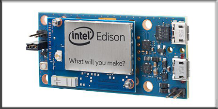
There are tech announcements, and then there are wait, hold on, come again? tech announcements. Intel Edison belonged firmly in the second category. When Intel pulled the curtain back on Edison in 2014, the pitch sounded almost suspiciously futuristic: a full Linux-capable computer, with wireless connectivity, squeezed into something close to the size of an SD card. In an era when the Internet of Things was still half buzzword and half science fair project, Edison felt like Intel was trying to shove the future into a pocket-sized rectangle and dare everyone else to keep up.
And to be fair, that was exactly the point. Edison was not meant to replace your laptop, your desktop, or even your Raspberry Pi in the broadest sense. It was designed as a tiny, low-power compute module for wearable tech, connected products, robotics, and fast-moving prototypes. Intel wanted inventors, startups, and makers to look at everyday objects and ask a dangerous question: “What if this thing had a brain?” Suddenly, baby onesies, dresses, mugs, bottle warmers, and robots were all fair game. Your coffee cup was not safe. Your jacket was on notice.
What Intel Edison Actually Was
At its core, Intel Edison was a computer-on-module built for the emerging world of embedded computing. The early version introduced at CES 2014 was described as a Quark-based system in an SD card form factor. That initial reveal was clearly designed to grab headlines, and it worked. The idea of a Linux computer that small immediately gave Edison a kind of sci-fi glow. It sounded like something a hardware hacker in a movie would slide into a mysterious port and use to unlock a satellite.
But the story got more interesting once Edison matured from flashy concept to shipping hardware. By the time Intel formally released the module later in 2014, the final Edison had evolved into a slightly different and much more practical product. It was no longer literally an SD card-shaped computer you would casually pop into a camera slot. Instead, it became a compact compute module measuring roughly 35.5 by 25 millimeters, with a 70-pin connector that opened the door to many more I/O options than an SD card-style design ever could. In other words, Edison grew up a little, and that extra space bought it real usefulness.
Why Intel Made Such a Tiny Computer
To understand Edison, you have to remember what Intel was chasing at the time. The PC market was still huge, but it was obvious that the next wave of computing would not live only in laptops and towers. Wearables were heating up, smart home gadgets were beginning to multiply, and developers were looking for modules that could add intelligence to small products without demanding the physical footprint of a traditional board.
Intel wanted a seat at that table. Edison was part moonshot, part market signal. It told the world that Intel was serious about wearables and the IoT ecosystem, and that it believed x86 could still matter outside traditional PCs. Instead of focusing purely on raw performance, Edison was built around size, connectivity, and flexibility. It was aimed at entrepreneurs building prototypes, inventors testing product ideas, and developers who wanted to combine Linux software tools with the kind of compact hardware usually associated with embedded systems.
That positioning mattered. Intel was not simply selling a chip; it was selling a shortcut from idea to prototype. If you were designing a connected fitness product, a smart accessory, a sensor hub, or some delightfully strange wearable masterpiece, Edison promised to reduce the distance between “what if” and “look, it boots.”
The Specs That Made Makers Pay Attention
For something so small, Edison packed a surprisingly serious set of features. The shipping module used a 22nm Intel SoC with a dual-core, dual-threaded Intel Atom CPU clocked at 500 MHz, paired with a 32-bit Intel Quark microcontroller running at 100 MHz. That combination mattered because it let Edison straddle two worlds at once: richer application-level computing on one side, and microcontroller-style device control on the other.
It also included 1 GB of LPDDR3 memory, 4 GB of eMMC flash storage, dual-band Wi-Fi, Bluetooth 4.0, and support for 40 GPIOs. For developers, that made Edison feel less like a novelty and more like a legitimate platform. It supported Yocto Linux, and Intel positioned it to work with familiar tools such as the Arduino IDE, Eclipse, and Intel’s own XDK. That meant a developer could think beyond blinking LEDs and start building connected products with real software logic, network access, cloud communication, and hardware control in the same package.
The module was tiny, but the ambition was not. This was a board that wanted to live in products, not just on workbenches. Intel also released supporting hardware, including a breakout board kit and an Arduino-compatible kit, which made Edison far easier to prototype with. Suddenly, the idea was not merely “here is a tiny computer,” but “here is a tiny computer you can actually build something with before your coffee gets cold.”
Real Demos That Sold the Dream
One reason Edison made such a splash was that Intel did not just wave the module around and talk about theoretical possibilities. It showed examples. At CES, one of the most memorable demos involved Rest Devices’ Mimo smart baby monitor system. Edison powered a connected baby onesie that tracked information like breathing and temperature, then passed that data to other smart objects in the environment. A bottle warmer could begin heating milk automatically. A connected mug could signal parents visually. It was equal parts useful, weird, and wonderfully CES.
That demo captured what Intel wanted Edison to represent: invisible computing embedded inside familiar things. The message was simple. The future was not one more slab of glass in your pocket. The future was intelligence quietly hiding inside objects you already used.
Later examples widened Edison’s image even further. The module appeared in prototype robots, experimental wearable fashion, Braille printing projects, and even research installations such as connected beehives. Intel and the maker community clearly enjoyed showing off Edison in projects that were part practical, part theatrical. One minute it was helping monitor infants; the next it was helping power a 3D-printed robot or a dramatic “Spider Dress” that reacted to people entering the wearer’s personal space. Subtle? Not always. Memorable? Absolutely.
Why Edison Felt Like a Big Deal in 2014
Edison landed at the intersection of several trends that were all gathering speed. Makers wanted more powerful boards. Startups wanted smaller hardware. Wearables needed lower-power platforms. And software developers wanted embedded devices that did not feel like exile from modern programming. Intel’s pitch was that Edison could bridge those needs.
In 2014, this sounded refreshingly bold. Raspberry Pi had already proven there was enormous appetite for inexpensive, compact computing. Arduino had made hardware experimentation more approachable. Intel’s move with Edison was to say: what if we mash together the tiny form factor of embedded hardware, the familiarity of Linux tools, built-in wireless, and enough horsepower for serious connected applications?
That was a compelling formula. Edison was not the cheapest board, nor the simplest. But it had a premium, high-concept appeal. It looked like a hardware platform built for the next chapter, not the last one. Even the aesthetics helped. The board looked sharp, modern, and unmistakably engineered as a product rather than a rough hobbyist compromise. It was the kind of module that made people say, “I’m not sure what I’ll build with this yet, but I suddenly want to build something.”
Where Intel Overpromised, and Where It Smartly Adjusted
No honest historical look at Edison should ignore the gap between the launch fantasy and the shipping reality. The original headline-grabbing “computer the size of an SD card” was a brilliant marketing hook, but it was also limiting. A product that tiny would have faced serious tradeoffs in connectors, shielding, expandability, and practical integration. Intel’s later decision to make Edison slightly larger was not a retreat so much as an admission that developers need a real platform, not just a miracle headline.
That redesign made Edison better. The 70-pin connector gave the module room to breathe. The Atom-plus-Quark combination made it more capable. The breakout and Arduino options made it more usable. From a product perspective, the evolution made sense. From a hype perspective, it also revealed how often emerging hardware launches are a dance between concept art and engineering reality.
Still, Intel deserves credit for shipping something interesting rather than leaving Edison as a permanent keynote prop. Plenty of flashy ideas disappear after applause. Edison actually became a tool that makers and developers could buy, test, and deploy. That alone gave it far more substance than many CES darlings ever manage.
The Business Side: Price, Ecosystem, and Target Audience
Intel priced the Edison module at around $50, with the breakout board and Arduino kit costing more. That placed it above some entry-level hobby boards, but Edison was clearly not aimed at casual tinkerers alone. Intel positioned it for expert makers, product designers, startups, and commercial prototyping teams. The company also worked to build an ecosystem around it through distribution partners and development support.
The strategy was smart. Tiny hardware only matters if people can actually use it, source it, and build around it. Intel highlighted support for Arduino and C/C++ first, then pointed toward Node.js, Python, RTOS options, and visual programming. SparkFun created Edison blocks. Maker-oriented distribution helped the board reach the people most likely to test its limits. This was Intel trying to meet the maker world halfway instead of expecting everyone to arrive wearing a corporate badge.
The Long-Term Legacy of Intel Edison
Edison did not become the default brain of the IoT revolution, and Intel eventually discontinued the module. In hindsight, that outcome is not shocking. The embedded market is brutally competitive, costs matter, tooling matters, and developer loyalty can be stubborn. Smaller, cheaper, and more specialized alternatives kept arriving. Some platforms were simpler. Others had stronger grassroots communities. And Intel, for all its engineering muscle, never fully dominated this particular corner of the maker universe.
But discontinuation is not the same thing as irrelevance. Edison mattered because it showed what a premium, tiny, wireless-enabled compute module could look like when a giant like Intel took wearables and connected devices seriously. It helped normalize the idea that a very small module could run Linux, handle connectivity, and sit inside products that did not look remotely like traditional computers. That idea is common now. In 2014, it still felt a little magical.
More importantly, Edison captured a transitional moment in tech culture. Hardware was becoming friendlier, prototyping was becoming faster, and the boundary between “object” and “computer” was beginning to dissolve. Edison was not the only reason that shift happened, but it was one of the products that made the shift visible.
Experience: What Intel Edison Felt Like to the Maker World
The experience surrounding Intel Edison was bigger than its tiny dimensions. For many developers and makers, Edison arrived like a challenge disguised as a gadget. It was small enough to spark immediate curiosity, yet powerful enough to make people think beyond hobby-grade experiments. The first emotional reaction was usually disbelief: That little thing runs Linux? The second reaction was ambition. Suddenly, people were imagining connected jackets, sensor-driven bikes, pocket robots, smarter home devices, and prototypes that did not have to be bulky to be impressive.
Part of the excitement came from the way Edison blurred categories. It was not just a microcontroller, and it was not exactly a mini PC in the usual sense. It sat in the middle, which made it feel unusually full of possibility. Developers could think in terms of applications, networking, cloud services, and data processing while still working with GPIO, serial interfaces, and low-level control. That hybrid identity gave Edison a kind of creative electricity. It invited experimentation from people who liked software, hardware, or both. It made embedded development feel less like a narrow specialty and more like a playground with real potential.
There was also a very specific thrill in the contrast between size and capability. The module looked almost too small to deserve serious attention, and that made every successful demo feel cooler. A prototype robot seemed more futuristic because the “brain” hiding inside it was barely bigger than a postage stamp. A fashion project felt more plausible because the computing hardware was no longer a giant brick strapped to fabric. A research device could become more elegant because the intelligence inside it stopped demanding center stage. Edison did not just compute; it disappeared into objects, and that invisibility was a huge part of its charm.
Of course, the Edison experience was not all cinematic wonder and triumphant demo videos. Real hardware work is messy. Developers had to think about breakouts, connectors, power, tooling, and the practical realities of integrating a tiny module into something useful. That is actually part of why Edison remains interesting in hindsight. It was a product that generated both admiration and friction. People were excited by what it could do, then quickly introduced to the ancient law of hardware: the smaller and smarter the board, the more carefully you must plan everything around it. Tiny computers still expect big patience.
Even so, Edison represented a valuable kind of optimism. It encouraged the belief that computing could become more intimate, less visible, and more imaginative. It suggested that intelligence could be woven into clothing, toys, medical devices, household objects, and research tools without turning them into clumsy mini-laptops. For startups and inventors, that was energizing. For students, it felt like permission to think bigger. For the broader tech world, Edison helped prove that the future of computing would not only be about faster screens and thinner notebooks. It would also be about objects quietly becoming aware, responsive, and connected.
That is the experience people remember most. Not just the board itself, but the feeling that almost anything could become a product category if the hardware got small enough and the software got flexible enough. Intel Edison may not have won the long game commercially, but it absolutely won a moment in the imagination of the maker movement. And sometimes that kind of win matters more than a clean sales chart. It changes what people believe is buildable. Once that happens, the industry rarely shrinks back to its old size.
Conclusion
Intel Edison was one of those rare hardware releases that managed to be both technically meaningful and narratively irresistible. It promised a computer nearly as small as an SD card, then evolved into a slightly larger but far more practical module for wearables, IoT products, robotics, and inventive prototypes. Along the way, it gave Intel a credible story in the embedded and maker space, while giving developers a platform that felt unusually ambitious for its size.
Did Edison completely reshape the market? No. Did it leave a mark? Absolutely. It helped push the conversation around tiny connected computers forward, and it turned the idea of “smart objects” from vague keynote poetry into something developers could actually buy and build with. In the history of small computers with oversized ambition, Intel Edison deserves a fond, slightly nerdy salute.